
A programme adopted a GaN platform, kept the original enclosure and discovered at the first thermal test that the design derated above two thirds of its rated output. The switching stage had been chosen; the design around it had not been planned, and the enclosure had been sized for the previous generation.
GaN charger design: the five stages to plan
The operating envelope, the switching frequency and the magnetics, the layout, the thermal path, and the certification that follows the change.
The stages are sequential in their dependencies and partly parallel in their execution: the envelope fixes the frequency, the frequency fixes the magnetics, the layout and the thermal path are developed together, and the certification work depends on how far the first four moved from the platform they started from.
A programme that plans the five stages can decide early whether it is extending an existing platform or developing a new one, which is the single decision that sets the calendar and the cost.
Stage 1: the operating envelope
Write the load profile, the ambient and the size target before the frequency is chosen.
The envelope states the continuous and peak output, the ambient at which the rating must hold, the port configuration and the enclosure volume available. On a GaN design the enclosure volume is the constraint that decides how much heat can be released, which makes it a design input rather than a packaging decision. An envelope written after the platform is chosen becomes a description of the platform rather than a requirement.
Stage 2: switching frequency and magnetics
The size advantage comes from this decision, and so does the electromagnetic work.
Raising the frequency allows smaller magnetic components and bulk capacitance, which is where the volume saving comes from. The same decision raises the switching losses per event and the emissions in the band the certification tests, so the frequency is chosen against the enclosure volume and the pre-scan margin rather than in isolation.
A design that keeps the previous frequency and changes only the device keeps the previous magnetics and volume while paying the device premium. The measurable output of this stage is the chosen frequency, the magnetics selected for it and the margin recorded at the pre-scan.
Stage 3: the layout
Faster edges put the layout on the critical path.
The switching loop, the gate drive returns and the sensing paths all have to be arranged for the transition speed, which is design work rather than component choice. A layout copied from a silicon design usually produces a higher electromagnetic signature and a temperature rise that appears at the switch rather than in the enclosure, so this stage is where the schedule is most often underestimated.
Stage 4: the thermal path
Less loss, less volume, and therefore a balance rather than a certainty.
The design has to move the remaining losses from the switching devices, the magnetics and the output stage through a smaller surface. The evidence is a temperature rise at full output in the shipping enclosure at a stated ambient, with the derating condition recorded. Where the design intends a smaller enclosure than the previous generation, the thermal result is the number that decides whether the size target is achievable.
Stage 5: the certification that follows
What has to be re-established depends on how far the design moved.
A new switching frequency changes the electromagnetic profile, so a pre-scan and often a new submission follow. A new enclosure re-opens the thermal and construction evidence. A change of magnetics or of the output stage is assessed against the tested construction. Planning the certification work as part of the design stages, rather than as a step after it, is what keeps the launch date inside the calendar.
| Stage | What it fixes | Evidence produced | Common underestimate |
|---|---|---|---|
| Operating envelope | Load, ambient, ports, volume | A written specification | The enclosure volume |
| Frequency and magnetics | Size, losses and emissions | The component selection and the pre-scan | The electromagnetic work |
| Layout | The switching loop and the sensing | A board revision | The time needed for a clean layout |
| Thermal path | How the losses leave the enclosure | The temperature rise at full load | The effect of a smaller volume |
| Certification | The evidence for the shipped revision | Reports and the construction review | How much has to be re-established |
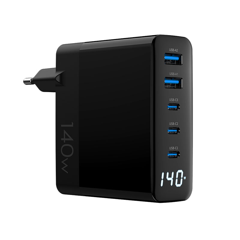
Extending a platform or developing a new one
The decision that sets the calendar.
Extending an existing platform is possible where the envelope fits inside the characterised range, the enclosure is unchanged and the switching frequency stays close enough that the electromagnetic evidence holds. Where any of the three moves, the programme becomes a development: a new board revision, a new pre-scan and, if the enclosure changes, a new thermal investigation. Naming which of the two the programme is, in the first week, prevents the schedule from being planned against the wrong shape.
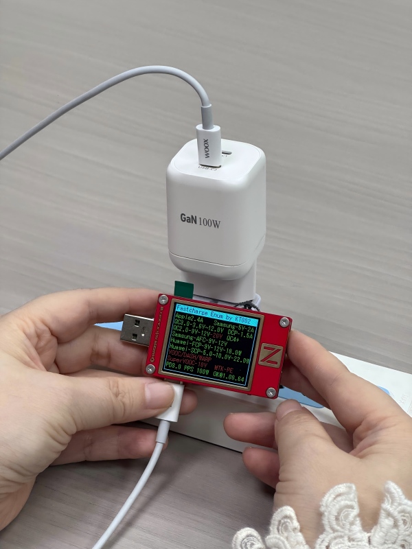
What to ask for at each stage
Five deliverables, and each is measurable.
The written envelope; the selected switching frequency with the magnetics and the pre-scan margin; the board revision with the layout changes described; the temperature rise at full load in the enclosure; and the certification position for the shipped revision. A supplier able to provide those five is running a design programme; one that provides the device datasheet is describing a purchase.
FAQ
Can a GaN design reuse a silicon enclosure?
It can, and the thermal result decides whether it should. The switching losses are lower and the volume is unchanged, so the design has more margin than the silicon equivalent at the same output; whether that margin is enough for a higher output is a measurement. It can, and the thermal result decides, because a lower-loss design at the same volume has more margin and the measurement says whether that is enough.
How much certification work follows a GaN change?
The electromagnetic profile changes with the switching frequency, so a pre-scan and often a new submission follow. A new enclosure re-opens the thermal and construction evidence, and a magnetics change is assessed against the tested configuration. The electromagnetic profile changes with the switching frequency, so a pre-scan and often a new submission follow, and a new enclosure re-opens the thermal evidence.
What is the most common schedule surprise?
The layout and the electromagnetic work. Both are engineering time that does not appear in a component list, and both sit between the design decision and the certification submission. The layout and the electromagnetic work are engineering time that does not appear in a component list, and both sit between the design decision and the certification submission. Ask for both as scheduled items rather than as assumptions.
Who owns the thermal evidence?
The factory produces it and the brand confirms that it matches the claim on the packaging and the product page. The measurement has to be taken in the shipping enclosure at the stated ambient, at full output. The factory produces the measurement and the brand confirms that it matches the claim on the packaging and the product page, taken in the shipping enclosure at full output.
Next step
Send the output range, the size target and the markets to Wecent Group through the contact page. The reply states whether the platform can be extended, the frequency and magnetics position, the thermal result in the enclosure and the certification work that follows. Related reading: GaN charger applications, OEM and ODM charger manufacturing and charger quality control. External references: USB Power Delivery specification, IEC standards, IEC Webstore, EU CE marking rules, UL standards and certification and TUV testing services.
{“@context”:”https://schema.org”,”@type”:”FAQPage”,”mainEntity”:[{“@type”:”Question”,”name”:”Can a GaN design reuse a silicon enclosure?”,”acceptedAnswer”:{“@type”:”Answer”,”text”:”It can, and the thermal result decides whether it should. The switching losses are lower and the volume is unchanged, so the design has more margin than the silicon equivalent at the same output; whether that margin is enough for a higher output is a measurement.”}},{“@type”:”Question”,”name”:”How much certification work follows a GaN change?”,”acceptedAnswer”:{“@type”:”Answer”,”text”:”The electromagnetic profile changes with the switching frequency, so a pre-scan and often a new submission follow. A new enclosure re-opens the thermal and construction evidence, and a magnetics change is assessed against the tested configuration.”}},{“@type”:”Question”,”name”:”What is the most common schedule surprise?”,”acceptedAnswer”:{“@type”:”Answer”,”text”:”The layout and the electromagnetic work. Both are engineering time that does not appear in a component list, and both sit between the design decision and the certification submission.”}},{“@type”:”Question”,”name”:”Who owns the thermal evidence?”,”acceptedAnswer”:{“@type”:”Answer”,”text”:”The factory produces it and the brand confirms that it matches the claim on the packaging and the product page. The measurement has to be taken in the shipping enclosure at the stated ambient, at full output.”}}]}